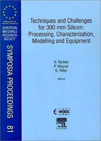
Techniques and Challenges for 300 mm Silicon: Processing, Characterization, Modelling and Equipment
G Ritter editor P Wagner editor H Richter editor
Format:Hardback
Publisher:Elsevier Science & Technology
Published:8th Sep '99
Currently unavailable, and unfortunately no date known when it will be back

The activities of the semiconductor industry to introduce a new, large wafer diameter were triggered by expected potential overall savings - cost and resource - and an anticipated increasing demand for Silicon wafers. In the beginning, around 1994, agreement on the diameter of the next wafer generation had to be achieved and finally 300 mm was globally accepted to be the next wafer diameter, a decision obtained at international summits in 1994/1995, based on the work of a SEMI task force. Several workshops on 300 mm wafers have been held by SEMI, JSNM and other organizations during the past few years. However, the present E-MRS conference on Techniques and Challenges for 300 mm Silicon: Processing, Characterization, Modeling and Equipment was the first international scientific conference about this subject. The papers - invited as well as submitted - cover a wide range of subjects, financial issues, fab concepts, crystal growth, wafer process development, material and defect issues, wafer characterization and provide an excellent review of the present status of 300 mm technology.
ISBN: 9780080436098
Dimensions: unknown
Weight: 670g
206 pages